
Homebrew Z80 Computer (Part 3)
I left the project in the previous post with a ROM on-board, but still running NOPs – it was running an EEPROM filled with zeros. The next step is to find a way to run programs and see the output. In order to do that I will need to do a few things:
- Add an STM32 ‘Blue Pill’ microcontroller to handle I/O
- Add an LCD display module to output debug information from the STM32
- Add a RAM chip, with some address decoding logic
I’ve also removed the diagnostic LEDs on lines A0 to A7 as they are no longer necessary and are taking valuable real-estate up on the breadboards.
Bill of Materials
In addition to the parts used in Part 1 and Part 2:
- 1 x STM32F103C8T6 “Blue Pill” microcontroller board – around £3 on eBay
- 1 x ST-Link V2 programmer – around £2 on eBay
- 1 x HD44780 16×2 LCD display with backlight – around £4 on eBay
- 1 x 628128 RAM chip – from around £4 on eBay
- 1 x 74HCD139 line decoder – less than £1 from most electronics suppliers
- 1 x 10kΩ Potentiometer (same as the one used in the timer circuit)
- 1 x 1µF Electrolytic Capacitor (to increase the clock frequency)
- 1 x 0.1µF Ceramic Capacitor (to decouple the RAM chip)
Schematic
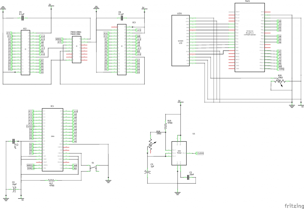
Changes from Part 2
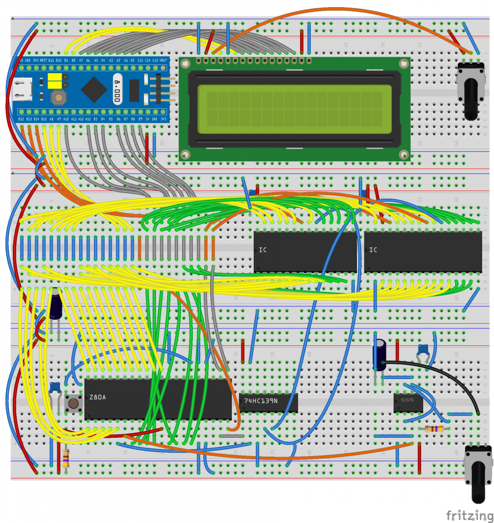
The most significant changes now are happening on the upper breadboards, but there are some other changes worth noting:
- The test LEDs, resistors and links have been removed.
- The timer circuit has been tweaked. There is now only a single 470Ω resistor alongside the pot. This can be taken from the pile removed when the test LEDs were removed. In addition, the 10µF Electrolytic Capacitors (C3) has been replaced by a 1µF part. This increases the maximum clock speed from 18Hz to 3.5Khz.
The additional changes to the board include:
- MREQ on the Z80 no longer goes directly to the ROM chip select, it is now connected to the input of the 74HCD139 along with A15 of the Z80. Two of the outputs of this logic chip are then connected to the ROM and RAM chip selects. If A15 is low, the bottom 32K of memory is being addressed, so the ROM is selected. Conversely, if A15 is high, the top 32K of memory is being addressed, so the RAM is selected.
- The Z80 IOREQ, RD and WR lines are now on the bus (orange wires)
- The STM32 is connected to the first 3 address lines of the Z80, the 8 data lines, IOREQ, RD and WR.
- The LCD display is connected to the STM32, with a potentiometer for controlling screen contrast.
- Power for the Z80 part of the circuit is now supplied by the STM32 via the USB port.
Important: Only power the board now from USB – do not connect to USB and an external PSU at the same time. The STM32 does not have any protection on the USB and it is likely that you will damage something.
Also, note that whilst the LCD is designed for TTL levels (5V), I’ve connected the data and control lines (grey and yellow) to 3.3V pins on the STM32. This is not an issue as those pins will be set to OUTPUT, and whilst the LCD input pins will be getting lower levels than expected, it is still within spec.
The STM32
The STM32 can be programmed using the Arduino IDE. In order to do this, a suitable bootloader needs to be installed so that it appears as a serial (COM) device when connected to the PC via USB, and can be programmed in future via the Arduino IDE over USB.
This is a one-off process.
- Follow the instructions here and download all the required files.
- Connect the STM32 to the ST-Link programmer via the 4 pins on top.
- Set the STM32 into program mode by setting the top jumper to position 1.
- Program the STM32 using this ST-Link utility.
- Set the top jumper back to position 0.
- Remove the ST-Link programmer and connect to a PC via USB.
- Run the mentioned driver utility install_drivers.bat if running Windows to fix the com port.
- Disconnect and reconnect the device from the PC USB. It should now appear as a COM port.
I will covered it with a full walk-through in a future post as it is not immediately obvious to the layman from searching Internet as to what the correct process is.
Address Decoding
The BSX has two memory chips wired to the data bus. The 74HCD139 decoder is used to ensure that only one chip is enabled at a time, and the correct chip is selected depending upon the address selected by the Z80.
I’ve decided to keep the BSX simple, with 32K of ROM between memory address 0x000 and 0x7FFF, and 32K of RAM from 0x8000 to 0xFFFF.
The easiest way to determine which chip I need to address is to examine the last bit of the address, or A15 on the Z80 address bus. If A15 is 1 (or high), then the Z80 is addressing our RAM area. If A15 is 0 (or low), then then Z80 is addressing our ROM area.
We can determine which chip to enable by combining the MREQ line and A15 using the logic built into the 74HCD139.
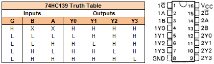
The logic chip has two sets of three inputs (G,B and A) and four outputs (Y0 to Y3). I use two of the inputs and two of the outputs. I’ve greyed out any results in the following table that can be ignored, for example GND as an input cannot be high by definition.
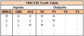
Pin B is connected to ground, so always low. G is connected to MREQ and A15 to pin A.
The output on Y0 will connect to the CS of the ROM, and is active low, so will enable the ROM if A15 is low.
The output on Y1 will connect to the CS of the RAM, and will enable the RAM if A15 is high.
Note that the RAM chip I’m using has two chip selects, one is active low, the other active high. I’ve connected Y1 to the active low chip select, and connected the second RAM chip select on the RAM chip to +5V, to pull it high.
Software
In order to make this board work, I needed to write three pieces of software. These are available, along with all the schematics in Fritzing format on my Github account. Note that this is a snapshot from 20th May 2020; later versions of the hardware require a UART to perform the serial communications and are not compatible with this board.
On the STM32
Code written in C that interfaces the board with the Z80 IO, with an interrupt driven off the IOREQ pin that responds to Z80 IN and OUT instructions.
At the moment this code forwards mainly keyboard data from the COM port (transmitted from a serial terminal package like Putty) and puts it on IO address 0, and passes back any output data, outputting it to the serial port (to b displayed in the terminal package) and the LCD screen.
In addition, the LCD screen displays the current address line the Z80 is addressing (from 0 to 7, as there are only 3 address lines connected to it), and the state of the RD and WR lines.
On the Z80
A simple Z80 monitor program in ROM that allows me to display the contents of blocks of memory in hex, load binary files into RAM, and jump to an address.
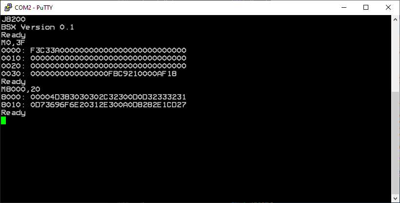
This code is compiled using sjasmplus and the binary file copied to the EEPROM using the MiniPro EPROM programmer used in the previous step.
In Powershell
A simple script to squirt a binary file down the serial port, with a header to tell the Z80 to start receiving binary data, the address in RAM to write the data to, and the length of the file.
This, combined with the minimal Z80 monitor ROM, will enable me to quickly test code in RAM without having to burn an EPROM each time.
Footnote
I had some issues with the LCD displaying garbage. At first it was wired up using only 4 data lines, so each byte had to be sent by the Arduino LCD libraries as two nibbles. I then wired it up using all 8 data lines, so each byte is sent in one go. That improved the situation, but didn’t completely fix it. I couldn’t find a suitable explanation from the electronics; all the voltages checked out. Finally fixed it by configuring the sketch to run at 48Mhz rather than 72Mhz (the STM32 default). That fixed the problem. The STM32 is significantly faster than the Arduino, so can only assume data is being sent too quickly to the LCD display. I will need to revisit the library at some point to see if I can fix it to work at higher CPU clock speeds.
What’s next
For the moment it will be mostly software. That notwithstanding, there are a few hardware tweaks that will need to be done sooner than later.
- Wire up the NMI (non-maskable interrupt) to a 50hz signal so that I can get a timer interrupt running on the Z80.
- Wire up a crystal oscillator clock circuit to replace the current 555 timer circuit so I can increase clock speeds a thousand-fold to 3.5Mhz (or above).
In addition, I will be looking at adding the following peripheral chips:
- A TMS9918 video chip for composite video output.
- An AY-8912 sound chip.
I will need to implement address decoding on the IO bus to do that, so that the STM32, TMS9918 and AY-8912 chips all appear at different IO addresses on the Z80 bus. At the moment I’ve only got one peripheral, the STM, on ports 0x00 to 0x07. To do that I’m going to investigate using reprogrammable logic chips (GALs) rather than discrete 74 series chips.