
Homebrew Z80 Computer (Part 2)
I left the project in the previous post running as a Z80 NOP test circuit; a minimal circuit for running a Z80 with no memory or I/O. The next step is to start fleshing out the board by adding an EEPROM.
Bill of Materials
In addition to the parts used in Part 1:
- 1 x 27C512 EEPROM (I used a Winbond W27C512-45 part)
- 1 x Minipro TL866II Eprom programmer (available from Amazon for around £40)
- 1 x 0.1µF Ceramic Capacitor (to decouple the EEPROM chip)
Schematic
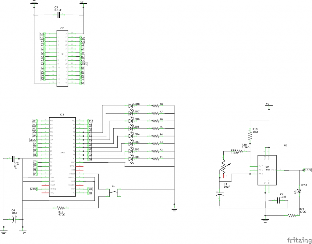
Changes from Part 1
The board has been transformed from the initial single-board layout in step 1 to one ready for future additions. Broadly speaking, the breadboards, from bottom to top, will be used for the following functions:
- Z80, clock and address decode logic for ROM/RAM
- Data and address bus, ROM and RAM
- Video and sound
- Power, I/O and overspill, in case I run out of space on the boards.
The breadboards are connectable, so can always add additional ones if I run out of space.
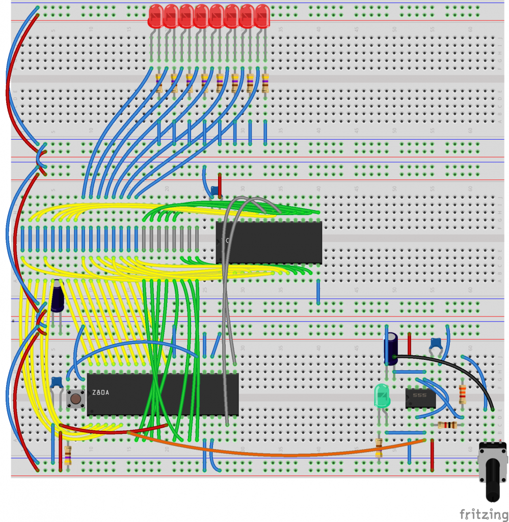
- The circuit has been rearranged on the breadboards to maximise use of space – the Z80 and timer circuit has now moved to the bottom breadboard, as it is highly unlikely I’m going to put anything underneath it.
- The address and data lines of the Z80 have been arranged in a bus on the breadboard above the Z80, with the 15 address lines (A15-A0) and 8 data lines (D7-D0) arranged in that order from left to right.
- The resistors below the Z80 pulling D7 to D0 and the link connecting MREQ to 5V have been removed.
- The LEDs have moved up the breadboard, and are now connected to the bus.
Adding the ROM
First, the ROM has been programmed in the EPROM programmer. By default, blank EPROMS are filled with 0xFF. In order to check this stage is working we need to fill it with 0x00 (NOP). This can be done in the EPROM programmer software by filling the buffer with 0x00 before programming the EEPROM.
Next, the ROM needs to be placed on the board next to the data lines. The following connections need to be made to enable it:
- A0-A15 to the address lines on the bus
- D0-D7 to the data lines on the bus
- CE (Chip Enable) to MREQ on the Z80
- OE (Output Enable) to RD on the Z80
- 5V and GND
As ever, double-check all the connections before connecting the power.
When running the LEDs will count in binary as per step 1. The only difference is that the Z80 is now executing NOP instructions from the ROM.
Footnote
I noticed that sometimes the Z80 will go a bit haywire when the power was applied – either not starting at address 0, halting with all the LEDs lit, or just putting seemingly random patterns on the address line LEDs rather than counting in binary. The reason for this is that really the Z80 reset line should be pulled low for a few clock cycles when power is first applied. This can be achieved with a resistor/capacitor circuit, or a 555 timer. For the moment I’m happy to just hit the reset button.
What’s next
The next step will be to assemble and run our first assembly language program on the ROM, and find a way for this program to output its results.