
Homebrew Z80 Computer (Part 1)
Designing and building my own 8-bit retro computer has been an ambition I’ve harboured for a few years now. I’ve studied and repaired a handful of computers of that era, and feel fairly comfortable with my electronics skills, yet have always considered designing a full system to be beyond the ken of normal folk.
After successfully building a Harlequin 128K, and chatting online to @6502Nerd, who has built his own homebrew computer based upon the 6502, I decided to have a crack at it.
The aim of this project is to build a fully functioning Z80 based computer inspired by, and hopefully compatible with, the MSX series of computers. Eventually it will boast:
- A Z80 running at 3.57Mhz
- 64K of RAM and 64K of ROM (both pageable and organised with a 32K/32K split)
- An AY-8912 sound chip
- Composite video output with sprites provided by a TMS-9918 video chip
- An STM32 ‘Blue Pill’ coprocessor to handle serial I/O, SD card reading, and debug output.
If you like what I’m doing, you can help support this project by contributing to my Ko-Fi page.
Bill of Materials
The kit of parts for this stage of the project are:
- 1 x 5V power supply – this needs to be exactly 5V for this stage
- 1 x Breadboard – I paid around £17 for a cheap one on eBay
- 1 x Box of link wires – I paid around £8 for a box of different lengths on Amazon
- 1 x Z80A CPU – Available for around £4 from RS Components
- 1 x 555 Timer
- 8 x Red LEDs
- 1 x Green LED
- 18 x 470Ω Resistors
- 1 x 1kΩ Resistor
- 1 x 3.3kΩ Resistor
- 1 x 10kΩ Potentiometer
- 2 x 10µF Electrolytic Capacitors
- 1 x 0.1µF Ceramic Capacitor
- 1 x 10nF Ceramic Capacitor
- 1 x Push Button
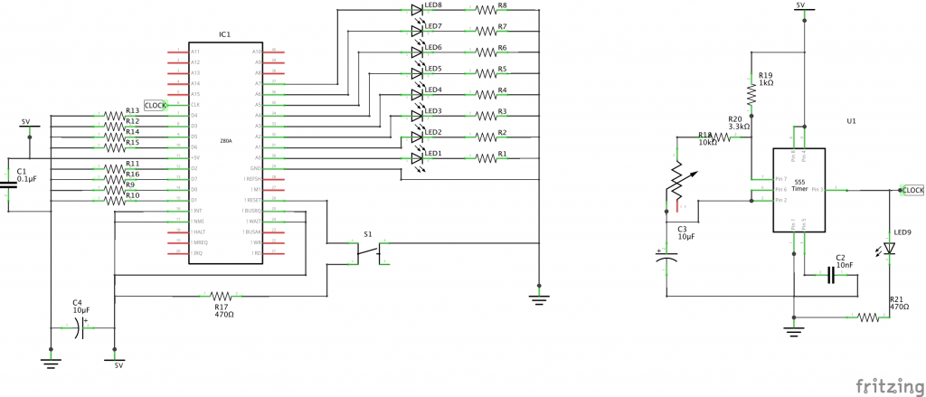
Schematic
The right-hand circuit is the 555 timer circuit, and the left the Z80 circuit linked via the <clock> symbol.
- S1 is the push-button switch that will ground the reset pin of the Z80 when pressed, triggering a reset. When open this will be pulled high to 5V via R17.
- C1 and C4 are decoupling capacitors to provide a smooth supply to the Z80.
- The 555 timer is connected via the label CLOCK to the RESET pin on the Z80.
Assembly
This project can be split into roughly two parts
The Clock Circuitry
Computers need a reliable clock signal – every action of the computer from running an instruction on the CPU, fetching data from memory and accessing devices is timed to this heartbeat.
Eventually the Z80 on this CPU will be fed a 3.57Mhz clock pulse from a crystal oscillator, but for the moment I’ve decided to slow things right down by using a 555 timer running in the region of 100hz, adjustable via a potentiometer.
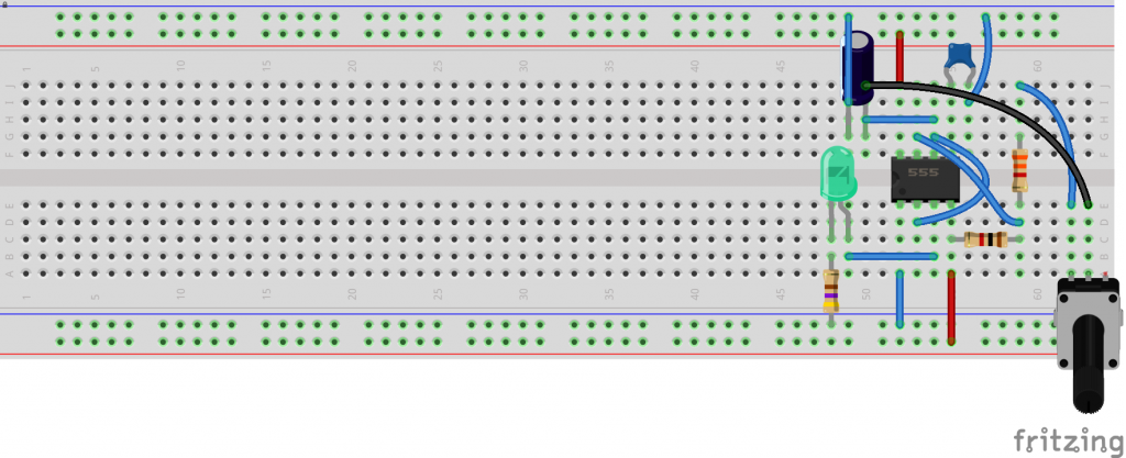
NB:
- I would advise putting the components in the same positions I have, as more components will be added later.
- The board requires a 5VDC power supply connected to the top and bottom power rails – blue (-) and red (+). If you watch my video, you’ll see my rails are swapped around. You may also need to put a short bridging connection mid-way along each power rail.
- The 555 timer is facing left, with pin 1 bottom-left.
- Note the polarity of the LED – if it does not flash, try putting it in the other way.
- The large 10µF electrolytic capacitor to the top-left of the 555 timer is polarised; the negative lead (indicated by the grey strip on the capacitor) must be on the left-hand side, connected to the blue ground line.
- The smaller 10nF ceramic can go in any orientation.
Once that’s been assembled, you should have a flashing green LED, who’s frequency can be altered by turning the potentiometer. If that doesn’t happen, disconnect the power and check your connections.
The CPU
Once that’s been tested, the CPU can be added
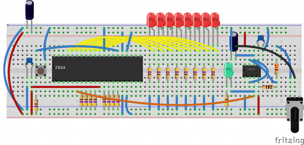
NB
- The reset button connection is critical – it should connect to 5V via the resistor underneath it when open, and to ground when pressed. I’d suggest using a multimeter on continuity to double-check this.
- Note the long orange wire connecting the clock line of the Z80 to pin 3 of the 555 timer.
- The Z80 is facing left, with pin 1 bottom-left
- The 10µF smoothing capacitor on the top-left of the board is oriented so that its negative lead is connected to ground.
When you run this, it should start counting in binary on the 8 red LEDs. If that doesn’t happen, disconnect the power immediately and check your connections. The left-most LED will flash when lit – this is normal and is indicative of the Z80 attempting to refresh DRAM (dynamic RAM). This will be discussed in more detail when I get around to connecting the RAM chip.
What’s happening
This circuit is commonly called a Z80 NOP Tester, and will run a Z80 without any memory or peripherals. How does this work?
- The 8 resistors underneath the Z80 are connected to the data lines D0-D7. These are normally connected to the memory circuitry and will be set high (1) or low (0) depending upon the data fetched. For this test, they have been pulled low to ground, so the Z80 will always see 0 on the data bus. This corresponds to the Z80 instruction NOP (No Operation).
- A handful of control lines have been pulled high (MREQ, NMI, INT, BUSRQ and WAIT). If these were left to float, it could trigger an unexpected bus request or interrupt.
- The bottom 8 address lines are connected to the LEDs.
- When powered, the Z80 will perpetually execute NOP instructions and display the current address it thinks it is running the instruction from on the LEDs, or at least the bottom 8 bits of that address.
* Thanks to Twitter user @CJHicks15 for discovering I’d not pulled the WAIT line high; it worked fine on my Z80 (as demonstrated in the video) but was causing his Z80 to halt occasionally. Schematics and diagrams have been updated as of 3rd November 2020.
What’s next
The next step will be to connect a ROM to the Z80 and attempt to run our first program.