Building a Harlequin Spectrum 128K Clone
This mini project was a good opportunity for me to practice my soldering skills, as well as get my hands on a Spectrum 128K clone that I could use for various projects.
I have enjoyed reading Chris Smith’s excellent articles on reverse engineering the ZX Spectrum ULA. The Harlequin is the physical embodiment of his work. The board comes in two variants; a 48K version (currently on revision G), and a 128K version (on revision 2D). Neither version requires a ULA; like the project Chris Smith breadboarded, they implement the functionality of the ULA using a number of 7400 series logic chips. This functionality includes:
- Generating the display
- I/O (tape, keyboard, and audio)
- Providing a clock signal to the Z80 CPU
I opted to build the 128K version, partly because I’ve already got a 48K Spectrum, but mostly for the extra features offered by the 128K machines; a Yamaha AY-3-8912 3-channel sound, the extra memory, and RAM/ROM paging facilities. It also has an option for a built-in Kempston joystick interface.
The printed circuit boards are available from many online sources, such as eBay or Sell My Retro. I opted for a kit of parts from ByteDelight, a retro computer online store based in the Netherlands. The kit cost £80.99 including delivery to the UK. I had done a quick back-of-the-envelope calculation and decided that I couldn’t get the kit of parts any cheaper that that, and it would save me a lot of time and effort.
I feel obliged to state at this point I am not affiliated with ByteDelight, nor am I being sponsored in any way to promote their website or this kit. I purchased from them after doing research online, and paid for it with my own money.
The kit took about a week or so to be delivered, and is really well packaged. It comes complete with the motherboard, and most of the parts required to build a functioning Spectrum motherboard, including chip sockets. It does not include a ROM (I assume for reasons of availability and copyright reasons), power supply, video cables, joystick socket or case.
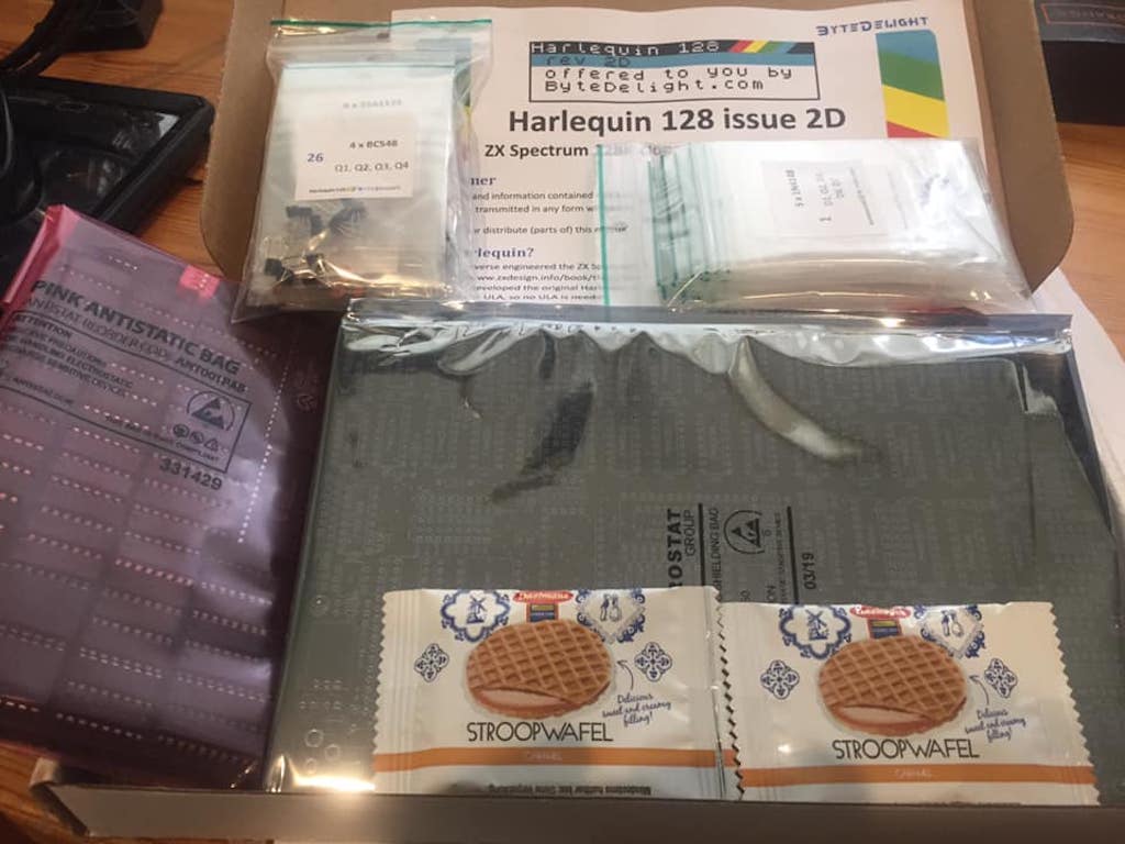
Tools required
- A fine tipped soldering iron; temperature controlled is a nice to have.
- A desoldering gun / tool / wick to fix any mistakes.
- A pair of side cutters for trimming component leads.
- A ROM, either salvaged from a 48K Spectrum, or a blank EPROM/EEPROM.
- An EPROM programmer if you decided to write out your own EPROM / EEPROM.
- Solder; about 25g, 0.7mm to 1mm diameter. I prefer 60/40 rosin core as it flows better.
Preparation
If you buy the kit from ByteDelight, there is very little to do in terms of preparation. All of the components are bagged and groups according to component value and build order, and the comprehensive build instructions provides many hints and tips on assembly.
I opted for a 29C040 EEPROM, because it is electrically erasable and it can store up to 8 sets of Spectrum ROMs selectable by DIP switch on the board. This part was a little tricky to get hold of. I ended up getting one on eBay for about £8. You can also use 27C256 or 27C512 EPROMs, but note that the 256 can only store a 256Kbit image (32Kbyte: 128K Toast Rack or +2), and the 512 a 512Kbit image (64Kbyte: +3). Also, EPROMS can only be erased with a UV EPROM eraser, making them slightly less convenient.
I already own a TL866+ EPROM programmer. These are widely available from online marketplaces for around £40, including the software. This can be used to program EPROMS and program/erase EEPROMS. I also have a cheap(ish) WEP 948 II soldering station bought from Amazon for about £200 with a temperature controlled soldering iron, desoldering gun, and hot air rework tool.
To add to my toolkit for this project I purchased an LCR-TC1 component tester. I do quite a lot of tinkering with retro computers, so figured this would come in handy at some point.
In addition, I used a plastic former for bending axial component leads, a multimeter (with continuity tester) to check for shorts, a magnifying glass, and a rubber soldering mat to protect my desk and provide a non-slip surface for the motherboard whilst I was working on it.
Assembling the motherboard
This is the largest hand assembled board I’ve attempted to date, so approached it with some trepidation. However, once the first few components had been soldered on, I quickly got into the swing of things.
There were a couple of times where the otherwise excellent build instructions could have been a bit clearer. These may have caught someone out who is less familiar with electronics components. However, on the whole the assembly felt no more complex than assembling an Airfix or Lego kit.
NB: Ben at ByteDelight has subsequently been in touch to say that he’s made some amends to the documentation – see my update at the bottom of this blog post.
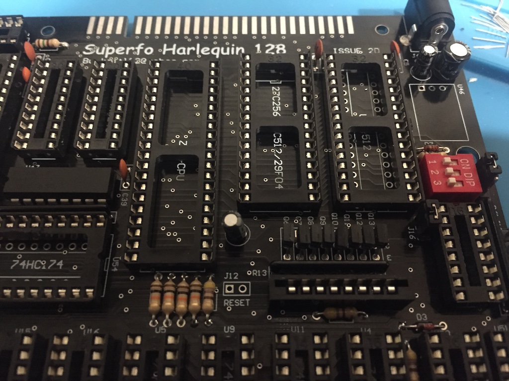
The first issue was with a block of 8 transistors assembled in-line above the right keyboard connector.
These transistors are flat, so it was difficult to tell the orientation from the accompanying picture in the manual
Fortunately I was able to use my new component tester. Popped one in to check, and confirmed it was the label side that was being displayed in the printed manual.
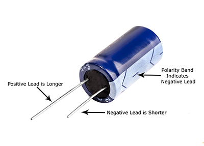
The second issue was to do with capacitors – it wasn’t entirely clear from the instructions how to identify the polarised capacitors.
Most of the capacitors on the board are small ceramic discs, but there are a handful of larger electrolytes, like the one in the picture.
A diagram like the one here could probably help some folk from making a rudimentary mistake and inserting a capacitor back-to-front.
But probably a fair assumption that someone tackling a build like this knows their way around basic electronic components.
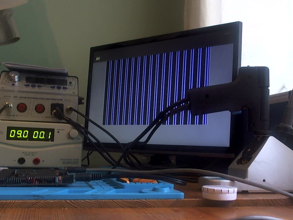
The third issue was in the ROM section. The first time I tested this Harlequin it failed to boot. It just displayed a screen with regular striping. It looked like the logic chips were displaying the screen, but something was amiss.
I spent a good hour checking the usual suspects, and then wondered whether it was the EEPROM at fault. It was at that point I experimented with the DIP switch, and discovered that the DIP switches select Bank 0 when all switches are ON, not OFF.
I’d only put ROM images in the first three banks on the EEPROM, so was trying to boot the Harlequin off an empty ROM in Bank 7 containing just 0xFFs.
These are all minor gribbles, and I’ve included them here for the record.
Assembly took a few hours spread over a number of evenings, starting with the diodes, then resistors, chip sockets, capacitors, and finally the transistors, sockets and chips. If you are unsure about soldering, or simply want a bit of a refresher, then check this comic strip out.
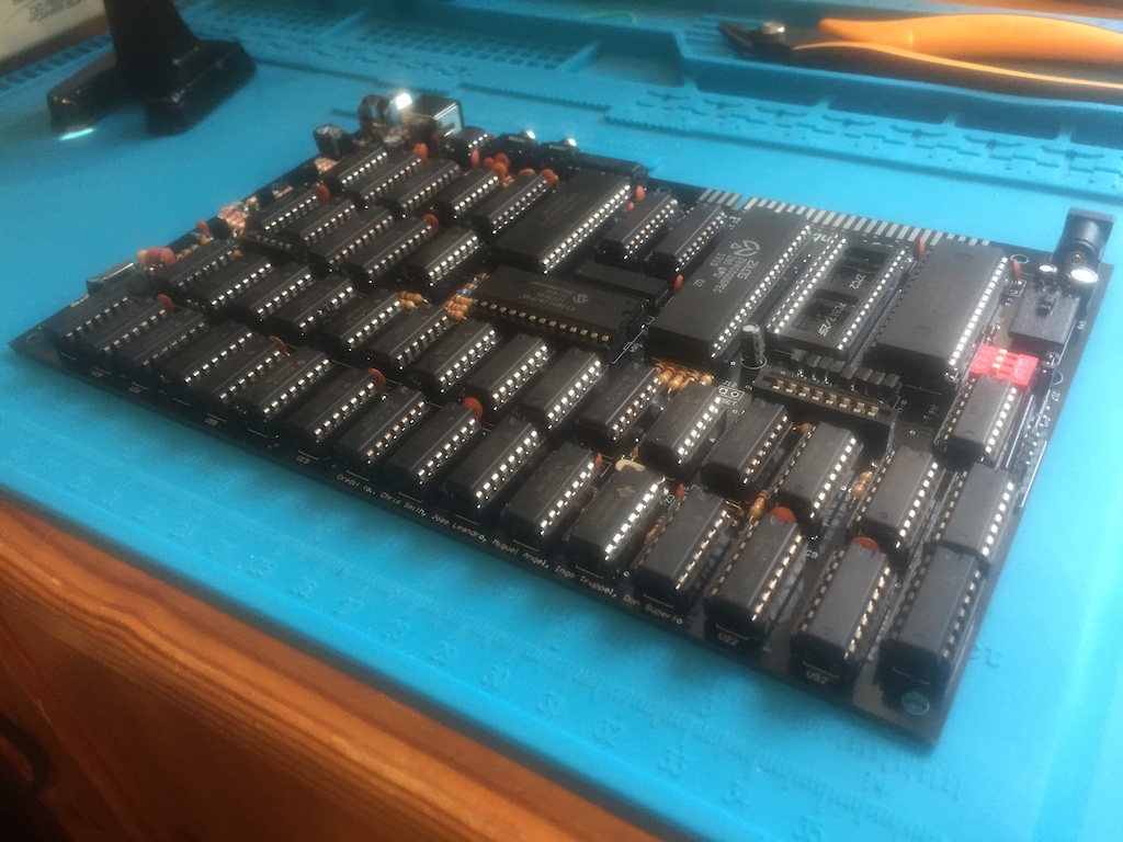
The board is very well designed, and the designers manage to cram a lot of components onto a board that is the same size as the Spectrum 48K board, even tucking a logic chip under the AY-3-8912 sound chip. This is also the only chip on the board that is not socketed, due to space restrictions, which makes ongoing maintenance a lot easier.
ROMS
I will spend more time going into the intricacies of ROMS, PROMS, EPROMS and EEPROMS in another article. Needless to say I have copied the following ROMS onto my Harlequin:
- Bank 0: Spectrum 48K (16K)
- Bank 1: Spectrum 128K Toast Rack (32K)
- Bank 2: Spectrum +2 (32K)
- Bank 3: Spectrum +3 (64K)
- Bank 6: ZX81 Emulator
- Bank 7: DiagROM
Banks 0 to 3 were simply burned from .ROM files that were supplied with my emulator (ZEsarUX). I’ve provided links for the ZX81 Emulator and the DiagRom. I may put the BBC Basic ROM on Bank 4, and leave Bank 5 free for my own projects.
The moment of truth
This was the moment I was kind of dreading – would it work first time? There are quite a few points of failure on a board of this complexity, and a lot of thoughts were running through my mind as I was preparing to power the Harlequin up for the first time:
- Is my soldering adequate?
- Have I put all the components in the right place?
- Are the transistors, diodes and capacitors in the correct orientation?
- Will there be any faulty chips?
- What if there is a manufacturing fault in the board itself?
I double-checked my soldering and chip positions before I applied power, and am glad, as I’d missed the solder on one side of a chip socket. These black glossy PCBs look lovely, but I find they make spotting soldering faults a little harder than more traditional green PCBs.
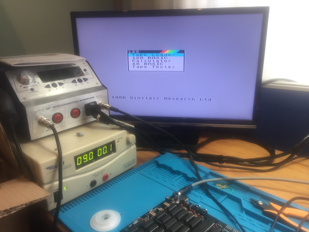
Needless to say, apart from that, and the aforementioned minor wobble caused by me selecting an empty ROM bank to boot from, the Harlequin did work first time. I’ve never been happier to see the Spectrum copyright message. Subsequent tests with a diagnostic ROM have all confirmed everything is working fine.
The Harlequin can connect to the TV via a standard RCA composite video cable (as I have in the above picture), or via the RGB connector using this RGB to SCART cable available from the ByteDelight website or other online stores. Note that there appear to be two variants of this cable; make sure you get the right one for your Harlequin PCB type. I’m certain the RGB cable will offer a far superior picture, yet the composite video output is still steady, clear, and with vibrant colours on my TV.
For power, I was using my trusty lab PSU set to 9vDC. As you can see, the Harlequin here is quite happy drawing around 100mA. You can purchase regulated power supplies for the Spectrum 48K from online stores for around £15, or use a Spectrum 48K PSU. The polarity is the same; centre polarity is -ve, the outer sleeve is +ve.
What next…
I will need to purchase a case and keyboard assembly at some point. These are available online from ZX-Renew. However, whilst testing this Harlequin with a borrowed Spectrum keyboard, I discovered the donor Spectrum had developed a fault, so may well leave the Harlequin in the borrowed case until I get around to fixing the faulty 48K motherboard that belongs there.
When I do get around to buying the Harlequin its own case, I will probably make the following mods:
- Add a joystick socket on the right-hand side of the case
- Mount a reset button on the back of the case near the composite video output
- Drill a hole in the back of the case so that the RGB connector is accessible
- Move the ROM select DIP switch to the back of the case, if there is room.
I have a project planned that requires an AY-3-8912 sound chip, but more on that in the future.
And going back to my opening paragraph about the ULA being implemented in logic chips, this board opens up the black box that is the Spectrum ULA, so will spend some time familiarising myself with the schematics, and probing all the logic chips with my scope to see how the Spectrum really ticks under the hood.
Finally, I’m just going to enjoy it. This kit has been a pleasure to build from beginning to end, and there’s nothing more satisfying than using a computer that you’ve assembled from a kit. There are quite a few 128K games that I’ve not been able to play up until now, so will be loading those up over the next few days and weeks.
Update: 11/03/2020
Just had a nice email from Ben Versteeg, the man behind ByteDelight – he’s looked at my comments and tweaked the documentation accordingly.
- Fixed a typo in the Jumper and DIP Switch Configuration section.
- Clarified the transistor photo and instructions.
- Confirmed that the ROM DIP switch logic is reversed; ON is 0 (tied to ground), and OFF is 1 (pulled up to +5ve)
Fab customer service!
Gallery
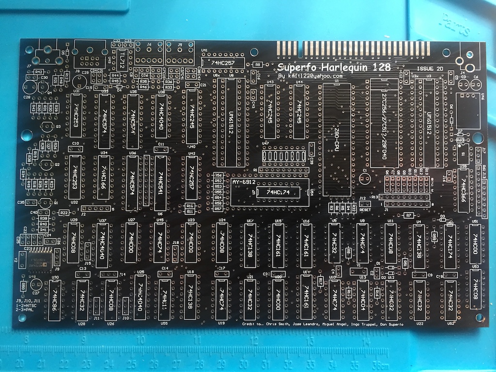
Unpopulated PCB 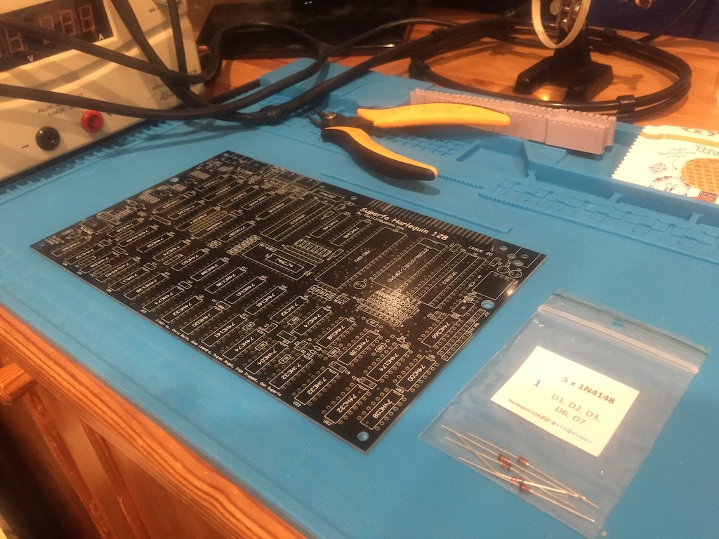
And so it begins 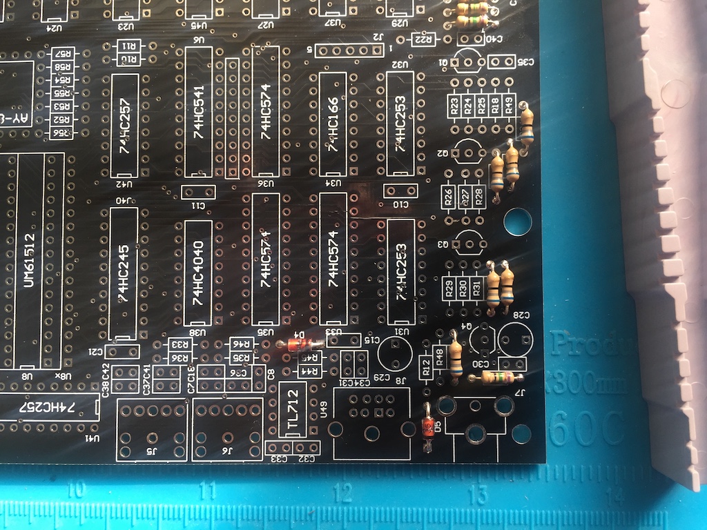
First components down 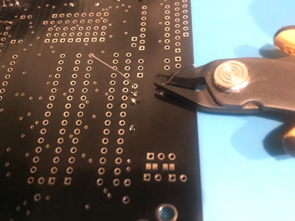
I usually snip before soldering 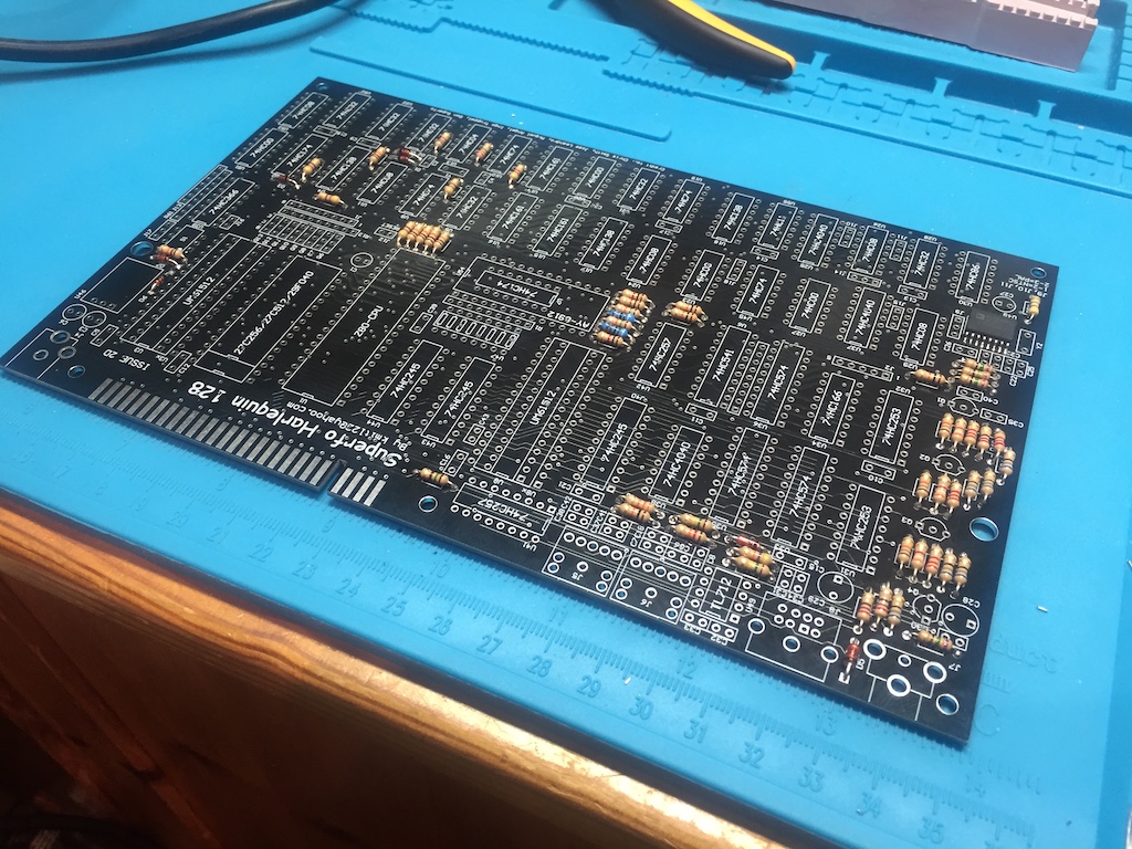
Diodes and Resistors all in 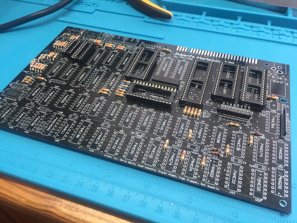
And now onto the socketss 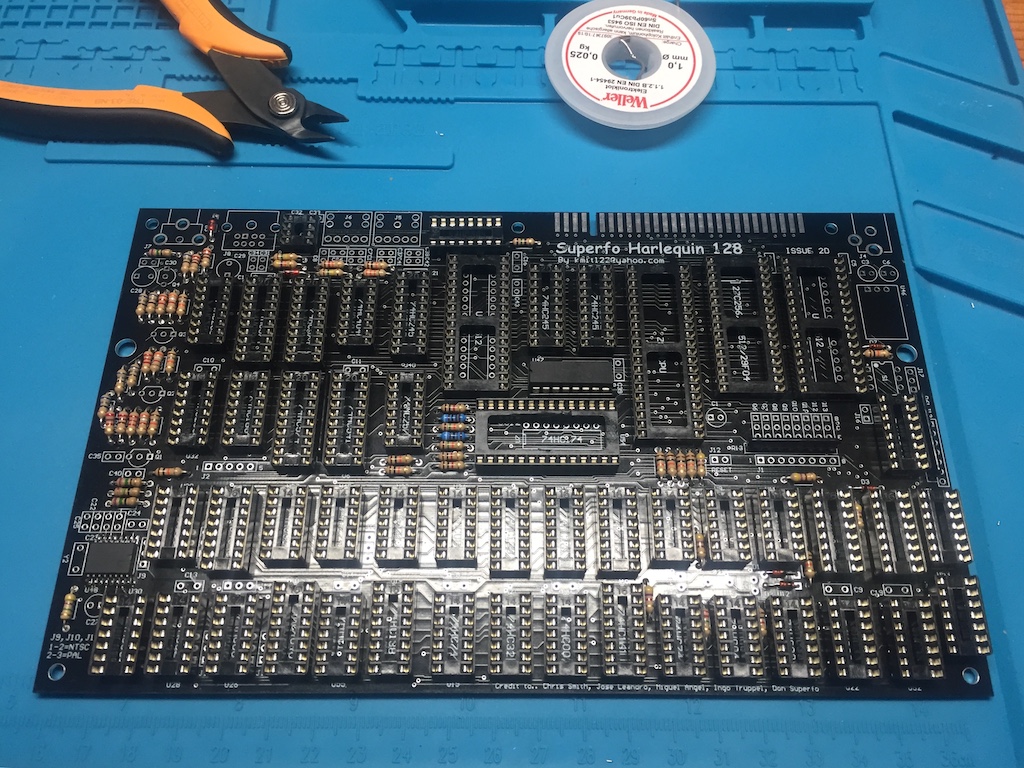
Sockets done 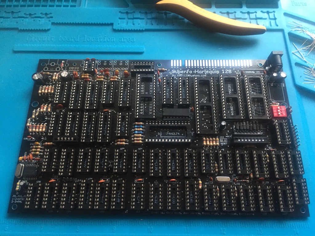
Onto the Capacitors 
And the keyboard connectors 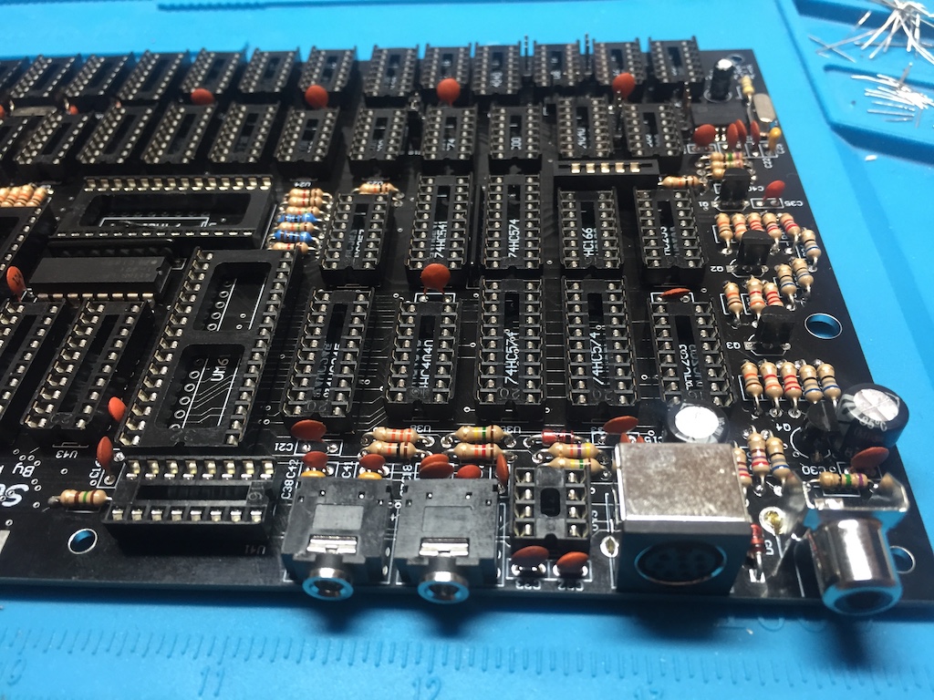
Video and Audio Sockets 
All soldering done 
Booting with 128K ROM 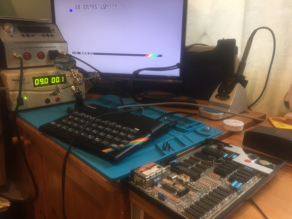
Testing with keyboard 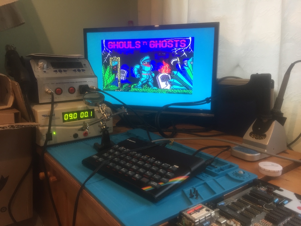
Loading a game 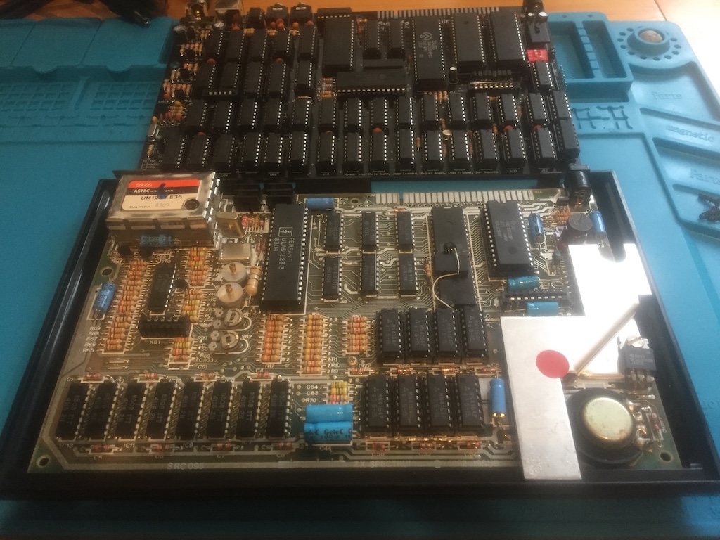
Old vs New
