Homebrew Z80 Computer (Part 5)
I decided quite early on in this project that I’d try to use interesting and contemporary technology to build the BSX, and make the BSX as simple to build on a breadboard as possible. The GAL is a perfect fit for all those criteria; it’s a technology I’ve not used before, it will cut the logic chip count down somewhat, and is a component that’s been around since the 1970s.
What is a GAL
A GAL, or Gate Array Logic is a programmable logic chip that contains an array of transistor cells arranged so that they can be configured to perform binary equations for each of the output pins based upon the state of the input pins. Unlike PALs, which are similar devices, GALs can be reprogrammed up to 100 times (according to the datasheets).
GALs are configured using a simple human-readable programming language called GALasm, and can be read and flashed by many common EPROM programmers, including the Minipro TL866II+, though your actual mileage may vary with older versions of the Minipro, or different brands of GAL.
Although GALs have been largely sidelined today by more complicated programmable logic devices such as CPLAs and FPGAs, they are still readily available, and are quite handy for TTL glue logic, such as address line decoding.
There are a couple of common GAL sizes; 16V8 and 22V10. The first two digits refer to the number of programmable pins, and the second the number of outputs. I’ll be concentrating on the ATF22V10C, though the principles are the same for smaller chips.
There are a handful of limitations:
- Pins 1 to 11, and 13 can only act as inputs.
- If the chip is to act as a latch, pin 1 is the clock pin.
- If any of the outputs need an output enable, pin 13 is the OE pin.
In addition, all pins have an active pull-up connection, and the chip has a security fuse that prevents configurations from being read, though this does not prevent the chip from being reprogrammed.
Why use a GAL
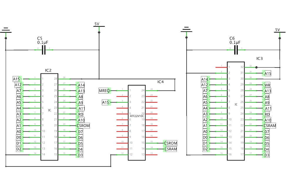
At the moment the BSX is using a single 74LS139 chip to decode the RAM and ROM chip selects based upon A15 (address line 15). This effectively splits the memory in half; the bottom 32K occupied by ROM. There is no further decoding of the address lines for I/O, so I would have to add more 74 series chips in order to select peripheral chips on the bus, i.e. UARTs, AY-8912 sound chips, and the TMS9918 video chip.
The GAL offers a better solution. I can have as inputs MREQ, IOREQ, A15, A14 and A7 to A0. And on the outputs I can have select lines for the various chips.
The logic for decoding the address lines can then be encoded in GALasm. For example, the logic to implement RAM and ROM decoding is as follows:
GAL22V10
BSX Address Decoder

MREQ 	IOREQ	A15	A14	A7	A6	A5	A4	A3	A2	A1	GND	; P01-P12
A0	RAMS	ROMS	NC	NC	NC	NC	NC	NC	NC	NC	VCC	; P13-P24

/RAMS	= /MREQ *  A15		; RAM select is low if MREQ is low and A15 is high
/ROMS	= /MREQ * /A15		; ROM select is low if MREQ is low and A15 is low

DESCRIPTION
Address line decoding for the BSX
RAMS: 	RAM CS (active low)
ROMS: ROM CS (active low)- The first line indicates the type of device, and it’s followed by a short description of the file.
- Two lines that label the pins, for use in subsequent equations.
- The output equations.
There are three operators:
- AND (*)
- OR (+)
- NOT (/)
So for RAMS (Ram Select), the equation is NOT RAMS = NOT MREQ AND A15, in other words if MREQ is LOW and A15 is HIGH, then set RAMS to LOW.
This GALasm file is compiled into a JED file for the EPROM programmer using a tool such as PALasm, or the one I use, which is GALasm. Note that this needs compiling to work on your target environment; this is fairly straightforward for Mac and Linux users, Windows users need to install the make tools.
I’m not planning on writing a guide on using GALs in all applications; there are plenty of examples on the Internet, but will recommend a couple of pages I found particularly helpful whilst researching GALs:
And the GALasm source includes a few good examples.
I will of course try to explain all GAL code I write as I expand upon its use in the BSX.
Implementing in the BSX
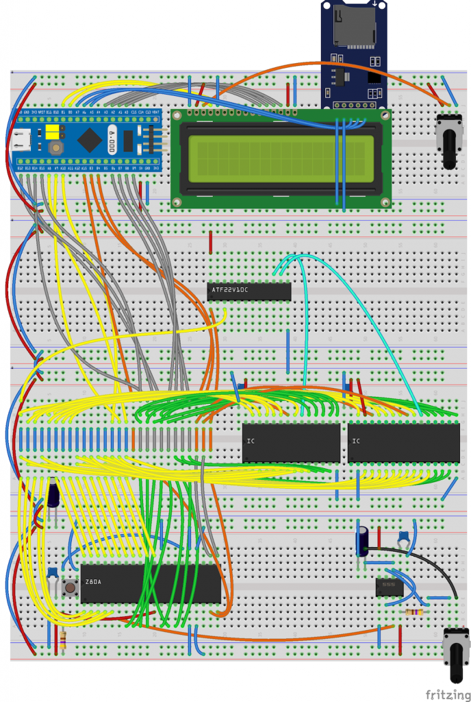
Fitting the GAL in the existing BSX circuit is fairly straightforward.

I’ve moved the GAL just above the memory chips, and removed the 74HCD139 logic chip that was situated between the Z80 and clock circuit at the bottom of the board.

What’s next
The next stage will be to implement a UART to take some of the load off the STM32 during communication between the Z80 and the PC. And once that is done, replace the 555 timer clock circuit with the crystal circuit I designed in part four ready for the TMS9918 video circuit.
